►
From YouTube: CHIPS Alliance - Advanced Interface Bus AIB Die to die PHY deep dive presented by Intel - 2021-08-10
Description
Download the slides: https://chipsalliance.org/wp-content/uploads/sites/83/2021/08/CHIPS_Alliance_AIB_Deep_Dive_081021.pdf
C
A
C
A
It's
a
great
pleasure
this
afternoon
to
introduce
the
aib
interface
that
intel
is
promoting
as
part
of
the
open
source
community,
along
with
blue
cheetah.
I
think
it's
exciting
technology
enables
an
entirely
new
world
or
ecosystem
of
design
and
thoughts
about
that,
and
so
with
that,
I'd
like
to
introduce
dave
kellett
and
have
him
introduce
the
team
today.
So
dave
and
I'm
recording
this
jim
by
the
way.
B
B
People
who
are
familiar
with
our
aib
journey,
we'll
recall
that
aab
was
invented
to
solve
a
die
disaggregation
challenge
we
had
with
the
stratix
10
fpga
on
the
previous
aria-10
generation.
We
had
a
monolithic
device
with
I-bandwidth
dye
connections
from
the
core
to
the
transceiver
columns,
as
shown
with
the
yellow
arrows.
B
When
we
selected
intel's
14
nanometer
process,
we
wanted
to
reuse
our
transceiver
design
built
on
tsmc.
The
immediate
question
was:
how
could
we
connect
the
fpga
core
built
on
intel's
high
performance,
digital
process
to
our
tsmc
process?
30's
designs
now
intel
had
earlier
invented
emib,
which
gave
us
7
8x
the
bandwidth
density
of
standard
packaging.
B
B
We
used
this
chiplet
capability
in
2018
to
add
56
gigabits
per
second
transceivers
to
stratix
10,
the
first
56
gig
transceiver
in
the
fpga
industry.
This
chiplet
capability
is
very
powerful
and
it's
attracted
the
interests
of
the
us
government
they've
sponsored
a
series
of
projects
from
darpa's
chips,
project,
the
navy's
ship
project
and
the
ramp
project,
I'm
showing
here
on
the
right
us
government
sees
chiplets
and
the
aib
standard
interface
as
part
of
their
formula
for
keeping
the
u.s
leadership
in
microelectronics.
B
B
B
D
D
D
So
what
I'm
showing
here
this
diagram
below
here
shows
an
example
of
an
fpga
based
system.
I
have
an
mcb
where
it's
or
a
multi-chip
package.
Within
the
package,
I
have
asic
talking
to
an
intel,
10
nanometer
agilex
fpga
over
a
die
to
die
connection
which
is
again
talking
to
another
chip
or
a
tile,
in
this
case,
ethernet
tile,
which
is
kind
of
interfacing
to
the
external
world.
And
this.
D
So
dave,
can
you
hear
me
somebody
muted
me
there
we
go.
Can
you
go
back
dave,
I'm
not
done
with
my
yeah.
This
mcp
can
go
on
on
a
board
which
is
again
interfacing
with
another
asic
and
that's
how
the
systems
are
built.
And
if
you
look
at
this
the
blocks
here,
they
are
again
connecting
over
a
standard
protocol
interface
next
slide.
D
So
there's
an
increasing
need
for
you
know
connecting
our
standard
protocol.
The
picture
on
the
right
shows
two
chiplets
over
connect
connected
over
a
v5
over
a
die
to
die
channel,
and
then
an
application
is
built
on
top
of
this.
Chiplet
customers
are
looking
for
a
solution
beyond
the
aib
file
they
want.
They
want
to
build
application
on
on
these
chiplets
and
when
you're
building
standard
application,
you
want
protocols
to
be
enabled
on
these
on
top
of
aib5.
D
So
what
we
have
done
here
is
we
have
created.
We
have
built
this
in
between
layer
to
enable
application
to
talk
over
standard
protocols
and
build
like
an
ip
based
system
on
these
applications
to
enable
like
an
end-to-end
connectivity
through,
and
we
wanted
to
do
this
over
a
standard
industry,
standard
interface
and
we
chose
axe
e4
for
that
next
slide.
D
So
now
I
I'll
jump
into
like
talking
about.
You
know
how
the
die
to
die.
Connectivity
is
usually
done.
There
are
two
broad
protocols
to
connect
between
die
to
die,
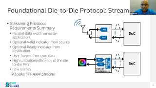
I'm
showing
here
a
streaming
protocol.
It's
the.
There
are
two
examples
that
I
have
on
the
right
side.
I
I'm
showing
like
an
adc
or
a
dac
converter,
connecting
to
an
soc
again.
This
is
like
your.
You
have
like
a
sensor,
a
converter,
sending
in
data
or
to
soc.
D
This
is
streamed
into
soc
and
I
can
there's
another
example
of
an
ethernet
optical
chip
over
over
a
transceiver
again.
This
is
connecting
to
soc
over
a
stream
interface
that
it
can
be
his
own
in
this
case,
like
an
ethernet
frame.
Going
into
this
to
see,
if
you
look
at
these
interfaces
right,
it's
it's
a
parallel
data
width
based
on
the
application.
The
size
can
be
different
and
usually
streaming
supports.
D
You
know
kind
of
varying
size
and
you
can
have
like
an
optional
valid
indicator
from
the
source
or
optional
ready
indicator
back
from
the
destination
to
to
provide
a
flow
control
again.
The
main
goal
is
to
keep
the
utilization
very
high
on
these
on
on
these
lines
here,
and
you
want
this
to
be
a
low
latency.
D
Here's
another
you
know
another
category
of
dietary
connectivity.
This
is
address
a
read,
write
where
an
example
would
be
like
a
memory
controller
talking
to
an
or
an
soc
talking
to
a
memory
controller
for
reading
and
writing
words
into
into
this
dram
array.
So
the
main
goal
is
for
efficiently
providing
read,
write
access
into
the
memory
controller,
and
this
is
exactly
what
the
axi
4
enables.
D
A
slight
variation
of
that
is
like
when
soc
want
to
read
and
write
into
the
control
status
register.
It
does
something
very
similar
to
axi
4,
but
it's
trying
to
economize
the
because
my
performance
doesn't
have
to
be
the
same
as
memory
controller.
I
can
economize
the
this
connectivity
and
do
like
a
you
know
like
a
low
performance
interface,
to
read
and
write
into
the
control
status
register,
and
this
is
exactly
what
the
x34
lite
does.
D
So
with
that,
you
know
what
we
really
want
to
do
with
when
I
say
providing
end-to-end
protocol.
What
what?
What
we
really
want
to
do
is
to
provide
this
type
of
interconnect
here,
so
I
have
a
chiplet
a
which
is,
which
is
an
asic
and
talk
into
a
soc
here
over
this
axis
to
aib
adapter
and
through
aav5,
connecting
or
ab5
and
within
that
soc.
D
D
Okay
next
slide,
so
now
I'll
go
a
little
deeper
and
talk
about
in
this
axi,
4
or
aib
that
we're
building
here.
So
I'm
showing
this
this
diagram
on
the
top
shows
an
axi
four
leader
and
an
axi
for
a
follower
here.
These
are
the
two
triplets
that
I
talked
about
on
the
on
the
initial
picture.
So
essentially,
what
we
are
trying
to
do
is
between
these
two
chiplets.
We
are
enabling
axe
for
and
what
we
need
to
do
in
between
to
to
do
that.
D
So
on
a
standard
monolithic
chip,
you
will
be
able
to
connect
between
the
leader
and
follower
and
you
will
have
the
ready
within
the
same
cycle,
be
asserted
when
there's
a
when
there's
a
request.
So
this
this
happens
kind
of
naturally
in
in
the
monolithic
chip,
but
when
you're
doing
this
across
die
to
die,
you
need
to
take
care
of
a
few
additional
things.
D
One
is
because
we
are
going
to
do
a
clock
forwarded
clock
based
clocking,
so
we
need
to
take
care
of
the
clock
phase
difference
between
the
leader
and
the
follower,
and
there
is
also
additional
delay
that
happens
between
the
blocks
that
we
are
connecting
to.
So
we
need
to
kind
of
also
handle
that
so
ends.
There's
a
need
to
build
this
axe,
e4
adapter,
to
kind
of
deal
with
some
of
the
die
to
die
characteristics.
D
D
D
Second
pitch
picture
here
shows
like
a
return
like
a
flow
control
back
from
the
follower
to
a
leader,
in
this
case,
like
a
credit
that
comes
back
from
the
followed
leader,
maybe
like
an
ethernet
frame
which
says,
I
know,
I
need
to
kind
of
flow
control
this,
and
the
third
example
is
basically
where
you
know
you
don't
you
you
don't
need
to
have
like
a
ready
or
valid.
You
can
just
keep
streaming
the
data
and
you
want
the
soc
to
kind
of
react
to
it
or
handle
this
without
any
ready
and
valid.
D
D
Basically,
you
know
you
will,
for
example,
if
you're
doing
like
a
write,
you
you
will
be
sending
the
right
address,
followed
by
the
right
data
and
there'll
be
a
right
response
coming
back,
so
you
need
to
kind
of
send
not
just
one
wire
or
one
set
of
data
you'll
be
having
you
know,
based
on
a
read
or
write.
You'll
have
more
than
one
channel
that
you
need
to
send
across
next
slide.
D
Here's
an
example
of
how
this
is
sent
across
right.
So
it's
it's
all
the
five
channels.
I
have
to
go
through
the
axi
four
adapter
to
a
b5
and
then
cross
the
wires
and
go
to
the
follower
on
the
follower
side.
Again,
you
recover
the
axis
four
adapter
recovers,
all
the
five
channels
and
presents
like
the
xc4
interface
to
the
follower
side
and
the
example
here
shows
how
a
write
data
is
actually
sent
across
to
to
the
leader.
D
D
So
that
would
be
the
axis
b4
and
I
didn't
talk
about
channel
alignment,
it's
included
in
my
slides
here.
Essentially,
you
need
a
way
to
align
the
data
on
the
other
side,
that's
another
ip
that
we
are
providing
all.
This
are
done
in
a
very,
very
configurable
way,
because,
based
on
the
application,
you
would
have
different
size
and
address
needs
so
there's
an
ip
generator
that
provides
this.
D
So
all
this
is
will
be
released
as
an
open
source
in
github
by
end
of
this
year,
and
we
will.
There
will
also
be
like
a
support
for
this
ip
for
next
for
three
years
after
the
release,
you
can
build
ip
with
with
this
and
if
there's
any
additional
capabilities
or
fixes
that
we
need
we'll
be
able
to
support
that
for
three
additional
years,
and
that
is
my
last
slide
here.
B
E
Dave
and
thank
you,
everybody
for
your
attendance.
My
name
is
krishna,
I'm
the
president
and
co-founder
of
blue
cheetah
today
I'll
be
talking
about
generators,
triplet
interfaces
and
aib
next
slide
all
right.
So,
to
begin
with,
I
think
it's
worthwhile
to
give
a
quick
overview
on
who
we
are
and
what
we
do
at
blue
cheetah
at
blue
cheetah.
We
specialize
in
the
development
of
what
we
call
as
generators.
E
Now
the
api
itself
within
the
bag
framework
is,
is
low
level
right.
So
it
enables
designers
to
create
design
procedures
and,
as
I
said,
it
enables
kind
of
rapid,
configurability
and
process
portability
as
well
to
develop
layouts
at
push
button
speed,
it's
worth
spending,
maybe
a
few
cycles
on
the
figure
or
the
diagram
on
the
right
hand,
side
of
that
slide
where
at
a
high
level,
you
know
the
framework
itself
is
kind
of
divided
into
three
levels.
Right,
you
have
the
circuit
generator
level
at
the
very
top.
E
So,
as
mentioned,
you
know,
designers
and
competent
designers
are
the
ones
that
develop
these
circuit
generators,
and
these
circuit
generators
can
take
in
performance
specs
as
inputs,
right
and
depending
on
what
the
designer
believes
needs
to
happen.
With
those
appropriate
performance
specs,
the
appropriate
design
can
be
created.
E
E
So
once
again,
this
is
what
we
call
as
our
generator-based
design
approach
and
as
mentioned
before
I'll
say.
Once
again,
you
know
we
believe
in
putting
the
designer
in
the
hot
seat,
and
so
we
capture
the
designer
knowledge
within
these
executable
generators
and
the
generators
themselves
are
only
as
good
as
the
designers
that
write
them.
E
E
E
On
the
other
side,
we
also
have
work
tremendously
on
memory
interfaces
as
well
right
so
specifically
on
lpddr4x
phi,
as
well
as
a
custom,
in-package
drm
variant
of
the
file
as
well.
Once
again
I'll
get
into
a
little
bit
of
the
details
here
in
the
next
couple,
slides
notice
that
the
the
the
projects
here
were
done
on
an
advanced
finfet
node,
and
it's
also
worth
re-highlighting
that
the
aib
generator
and
the
ams
circuit
generators
themselves
were
released
to
open
source
sometime
last
year
next
slide.
E
And
so
first
we
begin
with
a
little
bit
more
information
on
aib.
So,
as
mentioned,
blue
cheetah
developed
full
generators
for
all
of
the
the
custom
circuits,
things
like
drivers,
phase,
interpolators,
delay
lines,
etc,
leveraging
the
generator
technology
that
we've
been
pioneering
here
what's
very
exciting.
Is
that
not
only
are
those
generators
leveraged
for
open
source,
but
they
actually
help
produce
instances
on
intel
22ffl,
and
so
we
actually
had
silicon
proven
results
on
intel,
22ffl
technology.
E
Recently,
we
had
a
very
big
milestone
of
blue
cheetah,
where
we
actually
have
silicon
proven
results
of
our
memory
interfaces,
and
so,
in
this
particular
case,
generators
were
once
again
used
to
produce
fully
featured
memory
files
with
industry
standard
interfaces.
So
this
was
an
lpddr4
as
well
as
a
custom,
in-package
dram
variant
for
one
of
our
for
one
of
our
partners,
and
so
in
this
particular
case,
generators
were
used
to
assemble
the
five
circuit
blocks
themselves,
as
well
as
parameterized
assembly.
At
a
slightly
higher
level.
E
These
were
taped
out
on
advanced
finfet
nodes
and,
as
mentioned
over
the
past
couple
months,
our
team
has
been
working
very,
very
hard
to
get
the
silicone
proven
and
I'm
excited
to
say
that
this
actually
does
work
so
can
proven
right.
So
the
memory
interfaces
were
integrated
into
an
soc
and
the
full
soc,
along
with
the
interface,
showed
successful
operation
right.
E
It's
also
worth
noting
that
for
this
particular
project,
our
team
did
a
tremendous
amount
more
than
just
the
memory
interfaces,
so
we
actually
had
generators
for
plls
dc-dc
converters
as
well,
and
we
were
able
to
kind
of
tape
this
out
with
the
resources.
I
believe
that
we
had
partially
because
of
the
benefits
of
the
generator
flow.
E
Next
slide,
and
so
very
quickly,
just
going
back
to
the
chiplet
interface
space.
You
know
the
chiplet
interface
space,
as
I'm
sure
we
all
know
it's
a
hotbed
of
activity.
There
is
a
tremendous
amount
of
momentum
that
has
accrued
over
the
past
couple
years
and
it's
only
increasing
moving
forward.
So
there's
a
lot
of
adoption
by
not
only
the
us
government
but
tier
one
semiconductor
companies,
as
well
as
a
whole
slew
of
emerging
ai
and
edge
ml
startups
that
not
only
believe
in
the
cheaply
shifted
ecosystem,
but
want
to
embrace
triplet
interfaces
themselves
right.
E
But
if
we,
you
know,
look
at
this
space
holistically,
I
believe
the
triplet
interface
space,
at
least
at
this
time,
is
still
a
bit
of
a
wild
wild
west.
So
there's
a
number
of
different
standards,
a
number
of
different
packaging
technologies,
and
even
you
know
the
battle
between
closed
standard
versus
open
standard,
that's
all
kind
of
being
developed
and
pushing
forward
right
now.
But
the
key
thing
is
that
this
is
you
know
new
territory
and
something
that
can
potentially
be
very
profitable
for
a
lot
of
folks.
E
Now.
What
we
have
seen
is
that
there's
a
recurring
necessity
of
users
of
triplet
triplet
interfaces,
for
you,
know
rapid
configurability
and
ease
of
use
and
ease
of
integration
right
and,
in
fact,
aside
from
that,
there's
also
an
importance
for
state-of-the-art
power
performance
in
area,
so
making
sure
things
are
low.
Latency
area,
efficient
and
whatnot
is
also
very
important.
Faster
time
to
market,
especially
in
the
semiconductor
space,
is
a
universal
must
right,
that's
always
something
that
folks
require
and
obviously
reduced
risk
as
well
to
make
sure
that
things
are
actually
proven
and
working
accordingly
right.
E
So
we
believe
that
not
only
are
generators,
a
great
solution
for
that,
but
hopefully
the
next
generations
of
aib
can
really
fit
in
and
solve
these
problem
statements
as
well
right
next
slide,
so
my
final
slide
just
leaves
with
a
few
logistics
and
potential
next
steps.
If
folks
have
any
questions,
blue
cheetah
was
founded
in
may
2018.
E
We
are
led
by
globally
recognized
experts
on
the
analog
mixed
signal
side,
as
well
as
the
design
methodology
side.
We
are
a
global
team
now
of
25
employees
across
the
united
states
and
all
over
the
world,
and
we
are
full.
You
know
we
have
full
stack
expertise
at
the
company,
so
we
have
analog
digital
software
pdk
firmware
all
of
that
kind
of
under
one
roof,
which,
I
would
argue
is
precisely
the
skill
set
that
you
need
to
tackle
the
problem
statements
that
we
have
at
hand.
E
F
Hey
thanks
thanks
dave
for
inviting
me
to
do
this
forum
right
to
give
her
presentations
on
aipo
right.
I
somehow
couldn't
start
my
my
video
right.
So
sorry,
sorry
about
that,
so,
but
a
good
morning,
student
afternoon
to
everyone
in
the
car
right
depending
on
where
you
are,
I'm
I'm
like
one
from
intel
phd,
I'm
the
architect
for
aip
we're
focusing
on
defining
the
data
line,
solution
for
psg
I'll,
be
presenting
aibo
a
cost,
optimized
solution
for
the
ecosystem
today,
right
next
slide.
Please.
F
Here
are
the
outlines
of
today's
discussion.
I
will
start
off
with
some
dye
to
die
technologies
backgrounds,
then
moving
stewards
to
talk
about
afo
as
a
course
optimized
digital
internet.
I
will
also
go
over
the
aipo
bom
plan
and
the
consideration
that
associated
with
that
right.
This
is
to
show
how
we
could
achieve
the
bandwidth
density
through
the
innovative
package
property.
F
Next,
like
this,
this,
this
is
an
overview
of
the
dye
distribution
technology
that
is
widely
used
within.
The
industry
is
commonly
referred
to
as
a
2d,
2
and
half
d
and
and
3d
right,
usually
for
the
first
category,
which
is
what
people
usually
call
as
a
2d,
that
is
on
the
c4
and
it's
white.
It
has
been
used
in
a
multi-package
solution,
for
example
between
cpu
and
soc,
and
usually
it's
through
some
links
like
pcie
or
cxl.
F
When
people
talk
about
the
dye
distribution,
usually
what
we
think
of
is
the
microbomb's
immediate,
flicker,
interposer,
even
3d
right,
but
actually
all
this
can
be
used
as
a
as
a
technology
for
the
disaggregation
and
in
term
of
the
wire
density
right.
It
will
increase
from
2d
to
2.5,
ds
and
all
the
ways
to
3d
and
same
for
the
cost
as
well
right.
F
Next,
like
this,
okay,
the
the
right
hand
side
chart,
shows
a
different
generation
of
aid
and
and
its
data
rate,
as
well
as
the
bandwidth
density.
Aab
1.0
is
the
first
generation
here
right
or
it
can
be
referred
to
as
airb1
1.2
as
well
and
2
a
b
2.0
and
is
the
next
generation
right.
But
if
you
look
at
the
ab
2.0
and
right,
the
targeted
data
rate
is
the
same.
The
the
difference
is
really
on
the
channel
or
what
we
usually
refer
to
as
a
packaging.
Technology.
F
So
certainly
there
are
a
lot
of
application
that
doesn't
need
all
the
bandwidth
density.
That
airb2.org
provided
so
does
provide
an
interesting
solution
with
certain
bandwidth
price
point
power,
as
well
as
the
ease
of
manufacturing
right.
A
lot
of
the
vendors
out.
There
have
the
capabilities
to
manufacture
organic
substrate,
and
this
technology
has
been
measured
over
the
past
three
decades
and
one
key
thing
said.
F
F
It
can
support
both
a
b
2.0
and
natively.
The
the
five
will
be
designed
to
match
the
numbers
of
microbes
for
advanced
packaging
technologies.
By
changing
the
top
metal
layer,
we
could
rebump
to
c4
and
then
connect
the
different
numbers
of
ios
in
the
c4
versus
microphone
right.
In
this
case,
we
will
be
able
to
re
use
the
same
file
design
and
then
still
to
meeting
the
the
different
channel
design
channel
or
the
different
packaging
technologies
right.
F
One
key
aspect
we
we
we
need
to
keep
is
that
we
will
need
to
keep
the
channel
short
line
of
three
one.
Two
right.
The
arb
always
has
this
strong
line
that
this
is
the
key
for
us
to
enable
the
the
tablet
reuse
right
and
by
doing
by
enabling
the
the
aib
on
a
more
cost
optimized
organic
substrate
technologies.
F
The
tx
bank
fuels
is
at
the
nih
right
and
in
order
for
us
to
maximize
the
signal
density
and
and
still
maintain
the
the
shoreline,
the
china
shoreline
and
as
far
as
meeting
the
performance,
the
the
near
end
and
far
end
bunk
fields
are,
are
not
made
to
be
rotatable.
We
we
may
make
some
adjustments
to
the
bank
field
in
order
for
us
to
to
maximize
the
the
package
drafting.
The
next
slide.
F
I
will
show
some
diagram,
showing
is
how
we
managed
to
do
some
different
type
of
package
routings
to
meet
the
perform
to
meet
the
the
signal
density
right
and
so
for
for
a
chiplets
to
to
pair
with
itself
right.
Let's
say
for
for
debug
purpose
or
testing
purpose
right.
Some
data,
switzerland,
as
a
file,
will
be
required
and
and
the
clocks
are,
we
make
it
rotate
away
because
the
clocks
are
not
it's
not
something
that
can
be
easily
doing
the
swizzling
right
and
the
the
tables
on
the
right.
F
It
is
important
to
do
it
in
three
layers,
because
that
is
the
key
for
us
to
maintain
the
the
the
standard
form
pack
package
form
factor
of
five
to
five
layers.
Twelve
layers
right,
instead
of
increasing
to
more
and
more
leads.
Of
course
you,
when
you
increase
to
a
small
package
layer,
let's
say
from
12
layers
to
16
layer
or
even
20
layers,
then
you
can
pack
more
ios
and
you
can
pack
more
signals
per
channel
into
the
afo
right
that
the
spec
does
love
that
next
slide.
F
So
to
to
recap,
right
aipo
does
provide
a
cost,
optimized
dietary
interconnect
for
the
child
right.
That
is
the
main
three
driven
factors
for
for
us
to
look
at
apo
and,
and
we
will
be
able
to
utilize
a
single
file
to
skill
for
a
different
bandwidth
density
right
and
we're
trying
to
maximize
the
bandwidth
density
with
more
commonly
used
package
layer
right.
It's
not
like.
F
We
are
trying
to
do
it
with
a
new
package
layer
which
more
package
layers
and
or
new
technology
on
the
organic
package
that
will
defeat
the
the
purpose
of
the
introducing
appeal
of
because
we
want
it
to
be
a
more
cost
optimized
right.
That's
that's
all
for
my
discussion
today
right,
we
will
take
the
question
after
the
after
we
went
through
all
the
agenda.
B
G
G
As
like
one
said,
there
is
now
some
you
know
interest
in
going
vertical
in
terms
of
stacking
dyes,
and
there
is
an
increasing
use
of
3d
integration
outside
of
just
stacked
memories,
and
we
can
see
this
in
recently
published
material
specifically.
There's
an
example
that
I
listed
here
is
the
intellectual
processor
that
was
published
last
year
at
iccc,
and
that
is
a
logic
on
logic
type
of
platform.
G
And
so
people
are
typically
using
proprietary
or
simple
interfaces
and
then
not
really
going
outside
to
do
third
party
chipset
integration.
However,
this
is
going
to
change.
We
are
seeing
a
number
of
requests
for
integrating
third
party
chiplets
with
even
our
intel
ips,
and
there
has
been
some
demand
for
a
standard
interface
that
allows
you
to
do
this
in
a
very
nice
way
without
having
to
sit
together
and
design
the
entire
platform
together.
G
So
that's
what
we're
going
to
be
looking
at
specifically
today
now
one
of
the
nice
things
about
aib,
1.0
and
2.0,
and
that
they're
open
sourced
die
to
die,
fly
interfaces
and
then
they
do
enable
high
performance
interconnect.
So
we
want
to
leverage
them
as
the
basis
for
a
3d
open
source
standard
next
slide,
please
so
some
of
the
two
and
a
half
day,
diet,
type
by
standards
that
are
out
there.
I've
listed
some
of
them
here,
not
all
of
them.
G
But
you
know,
the
top
line
is
is
highlighted,
show
what
the
best
possible
energy
efficiency
we
can
get
out
of
these
standards.
But
for
this
eye
chart
I
really
want
to
highlight
the
aib
2.0
interface,
and
you
can
see
that
there's
a
very
nice
feature
to
aib
is
that
it
is
what
I
call
a
soft
macro
that
can
be
turned
into
a
hard
macro.
It's
a
gender
generator
based
analog
mixed
signal,
plus
behavior
rltl
design
that
can
go
across
different
process
nodes.
G
F
G
Just
emib
packaging,
but
you
know
over
interposer
and
other
types
of
dietary
integration
fabrics
and
then
the
other
nice
thing
is
that
it
is
open
source.
So
we
do
do
desire
a
similar
feature
set
as
the
2d
interface,
and
on
top
of
that
you
know,
aib
is
familiar
now
to
many
people,
and
so
basing
it
on
aib
2.0
is
something
that
we
do
want
to
do
next
slide.
Please.
G
So
here
what
I'm
showing
is,
first,
you
know
what
is
out
there
in
terms
of
3d
phy
interfaces.
Now
the
list
is
is
starting
to
grow.
There's
a
lot
of
memory
based
interfaces,
as
you
already
know,
and
then
there's
some
new
ones
coming
online.
A
lot
of
them
are
in
the
early
stages
or
not
open
source.
One
example
is
a
g-link
3d
from
guc,
it's
very
specific
to
tsmc's
packaging
technology,
and
it
is
not
open
sourced.
You
have
to
purchase
the
hard
macro
from
them
and
also
it's
very
early
stage
now
for
us.
G
What
we
want
to
do
is
we
want
to
be
able
to
support.
As
you
see
in
the
figure
to
your
to
your
left
on
the
top,
we
want
to
support
an
over
die
type
of
integration
of
the
phi
standard
and
also
on
the
shoreline
like
we're
used
to
with
with
our
two
and
a
half
d
standards,
and
we
want
this
to
be
scalable
across
a
wide
range
of
micro,
bump
and
tsv
pitch,
and
this
is
just
for
future
proofing.
G
The
standard
and-
and
you
can
see
in
in
the
bottom
picture
here,
it's
a
snapshot
taken
from
a
slide
that
was
presented
at
forum
five
in
icc
2021
by
imek,
and
you
can
see
that
you
know
there's
a
very
wide
range
of
pitches
that
are
listed
here,
going
all
the
way
from
a
3d
sip,
all
the
way
to
3d
ic.
Now,
obviously,
we
may
not.
G
We
probably
don't
need
a
standard
for
3d
ica
when
we're
just
stacking
transistors,
but
for
some
of
the
other
you
know
types
of
3d
integration,
it's
quite
possible
that
a
standard
would
be
required.
If
you
want
to
integrate
some
third-party
ip
with
your
own
design,
we
want
to
be
able
to
allow
half,
duplex
or
full
duplex
operation,
half
duplex,
primarily
because
we
do
see
that
you
know
in
case
somebody
wants
to
integrate
a
single
port
memory.
G
G
B
G
So
it
is,
is
what
I
call
a
soft
macro
and
then
the
other
important
thing
here
is
that
we
want
to
be
able
to
enable
some
non-intrusive
power
delivery,
and
this
is
something
still
very
early
stages.
It's
just
at
the
thought
level
where
you
know
intel
has
announced
some
very
interesting
new
3d
integration
technologies,
where
you
can
do
power
delivery
from
top
side
and
through
the
side
channels,
as
shown
in
this
picture,
where
you
don't
necessarily
have
to
drill
holes
through
your
base,
die
to
get
to
the
top
die.
G
So
this
is
a
high-level
picture
of
what
we
envisioned
the
architecture
to
be.
It
is
a
2d
array
of
various
signal
bumps
and
we've
shown
how
we
might
intersperse
power
and
ground,
and
this
is
just
concept
only
for
now.
We
obviously
may
with
some
further
analysis.
We
may
change
the
way
that
we
do
the
power
and
ground
bump
out,
but,
as
you
can
see,
we
can
scale
this
array
depending
on
on
bump
pitch.
G
G
G
G
So
if
you
wanted
a
larger
patch,
you
could
use
multiple
of
these
modular
patches
and
put
them
together
and-
and
we
can
we'll
sort
of
specify
how
you
might
do
that
in
terms
of
both
power
and
ground
distribution
and
also
clock
distribution,
and
then
we
also
want
to
be
able
to
configure
the
number
of
channels
next
slide.
Please.
G
So
you
can
see
that
the
tx
clock
is
is
sent
through
to
the
base
die
and
actually
180
degrees
out
of
phase
and
as
it
is
received
on
the
onto
the
base
die,
which
is
the
peripheral
dye.
A
dll
is
used
for
phase
alignment
so
that
the
clock
is
edge,
aligned
and
that
edge
aligned
clock
is
then
used
to
latch
or
flop
in
the
data
from
the
transmitter,
which
is
the
controller
die
to
the
receiver,
which
is
the
peripheral
die.
G
G
G
On
the
on
the
top
two
pictures
you
can
see,
the
intel's
recently
announced
at
fort
ross,
omni
and
focus
direct.
These
technologies
were
also
presented
at
intel
architecture
day
in
2020,
and
what
these,
what
these
technologies
allow
you
to
do
is
to
do
power
delivery
in
a
way
that
it's
not
intrusive
to
to
the
base
die.
You
don't
have
to
make
swiss
cheese
out
of
your
face
dies.
You
can
actually
using
pro
versus
omni,
which
is,
on
the
right
hand,
side
at
the
bottom.
G
You
can
actually
deliver
the
power
in
between
the
base
dies
that
are
shown
here,
the
memory
and
the
a6
using
the
larger
bumps,
as
shown
in
the
top
picture,
and
then
on
the
the
left
hand
side
at
the
bottom.
You
can
see
that
phobos
direct,
which
has
been
recently
announced
by
intel,
allows
you
to
deliver
power
from
both
sides
of
the
die
so
from
the
top
and
the
bottom
of
the
die,
and
so
this
is
a
very
nice
feature
where
it's
completely
non-intrusive
to
the
entire
packaged
system.
G
Next
slide,
please!
So
in
summary,
we
are
starting
to
draft,
you
know
aib3d,
and
we
are
seeing
an
increasing
use
of
3d
integration
outside
of
just
stacked
memories,
the
chiplet
ecosystem.
Really
we
want
to
increase
it
in
the
vertical
direction.
It
does
require
these
standard
interfaces
and
we
want
to
leverage
as
much
as
we
can
from
our
previous
work
on
aib,
1.0
and
2.0,
and
make
sure
that
the
aib3d
standard
is
also
open
sourced
and
it
is
flexible
across
process.
G
C
My
talk
is
about
how
the
aib
based
chipotle
ecosystem
has
really
helped
intel,
innovate
its
fpgas
in
ways
that
would
not
have
been
possible
or
would
have
been.
You
know
much
more
difficult
had
we
not
taken
advantage
of
it
and
I'm
going
to
be
taking
a
much
higher
level
of
view
than
the
prior
presentations,
but
I
think
it
will
really
help
to
see
you'll
help
you
to
see
the
benefits
we've
gotten
from
this
approach,
so.
C
We
have
built
all
the
members
of
our
stratix
10
series
shown
in
the
middle
there,
and
also
our
latest
fpgas,
the
agilex
series
shown
in
the
upper
right
so
pursuing
this
chiplet-based
methodology
has
helped
us
to
develop
and
deliver
many
industry-leading
capabilities
in
our
products.
In
particular,
in
agilex,
we've
got
a
45
performance
improvement
compared
to
our
prior
generation,
up
to
40,
lower
power,
pisa,
express
gen,
5
interfaces,
compute
express
link
interfaces,
transceiver
data
rates
up
to
116
gigabits
per
second
and
high
performance
integration
of
hbm2e
memory.
C
C
So
as
an
example,
let's
take
a
look
at
how
we
use
this
method
to
actually
build
the
stratix
10
fpgas,
our
stratix
10
gx
devices
consist
of
the
chiplets
highlighted
in
the
green
boxes,
including
a
14
nanometer
fpga
fabric
pci
express
gen,
3
and
28
gigabit
per
second
serial
transceivers
and
the
result
is
a
sort
of
a
general
purpose:
high
performance,
fpga
family
that
supports
pcx
best
gen
3
and
transceiver
data
rates
up
to
28
gig
next
slide.
Please.
C
Stratx10Sx
devices
are
intended
for
applications
that
need
an
integrated
processor,
so
for
this
family
we
use
a
14
nanometer
fpga
fabric,
with
an
integrated,
hard
processor
subsystem
or
hps.
As
you
can
see
there
in
the
the
box,
highlighted
the
green
highlighted
box
on
the
left,
while
keeping
the
interconnect
tiles,
the
ones
you
see
in
the
middle,
the
same
next
slide
in
the
case
of
our
stratix
10
tx
devices.
C
C
Our
next
stratix
10
family
is
targeted
at
applications
that
are
requiring
the
highest
memory
bandwidth.
So
we
integrate
a
stack
of
hbm
memory
and
continue
to
use
the
same
core
fabric
and
transceiver
chiplets
that
we
saw
before
so.
You
can
see
our
sort
of
a
repeating
theme
here,
we're
reducing
our
engineering
risk
and
development
effort
by
using
technology
that
was
proven
out
in
prior
stratix
10
families,
and
then
we
enhance
it
with
more
application.
Specific
functionality,
using
whatever
node
process,
node
and
foundry,
is
best
suited
for
those
functions
next
slide.
C
So
now
we
can
see
we've
added
a
pci
express
gen
4
capability
in
our
stratix
10
dx
families,
as
the
one
I'm
talking
about
now.
These
were
the
first
to
offer.
Fpga's
first
offer
that
were
certified
by
the
ap
express
special
interest
group
for
gen
four,
and
you
can
see
that
we
replaced
the
chiplet
that
provided
gen
3
capability
with
a
new
chiplet
that
provides
a
gen
4
capability
and
also
added
support
for
upi.
C
We
also
have
an
hbm
option
to
address
high
memory,
bandwidth
applications
and
we
kept
using
the
higher
speed
transceivers
to
support
the
correspondingly
higher.
I
o
bandwidth.
So
next
slide,
please.
So.
In
our
most
recent
stratix
10
family
called
stratix
10
nx,
we
used
a
new
fabric,
an
ai
enhanced
fpga
core
fabric,
along
with
the
58
gigabit
transceiver
chiplet
and
hbm
memory
that
we
introduced
in
the
prior
stratex
10
families
to
offer
intel's
first
fpga.
C
Next
slide,
please
so
following
stratix
10
we've
continued
this
chiplet-based
methodology
in
the
development
of
our
agilex
fpgas
and
the
agilex
fpgas
feature
an
fpga
fabric
that
is
built
on
the
10
nanometer
super
fin
process.
So,
for
example,
I'm
showing
you
our
f
series,
agilex
f
series
devices
where
we
have
paired
that
10
nanometer
superfin
core
fabric
with
chiplets
that
support
pci,
express
gen,
4
and
transceivers,
supporting
up
to
58
gigs
per
second
data
rates
next
slide.
C
The
other
agilex
series
shown
here
is
the
I
series
and
we
use
the
same
10
nanometer
superfin
fpga
fabric
chiplets,
as
in
the
f
series
that
I
just
showed
you
but
paired
now
with
different
combinations
of
interface.
Chiplets,
this
time
providing
pci
express,
gen,
5
compute
express
link
or
cxl
and
transceiver
data
rates
up
to
116
gigabits
per
second,
so
to
provide
even
more
differentiated
capabilities
that
are
targeted
for
different
applications
compared
to
our
f
series.
C
So
in
this
way
you
can
see
that
chiplet-based
design
has
really
enabled
us
to
introduce
new
technology
rapidly
by
building
on
a
firm
foundation
of
existing
chiplets
and
then
mixing
and
matching
those
chiplets
using
any
combination
of
ip
process.
Node
and
foundry
to
achieve
the
specific
functionality
required
next
slide.
C
C
C
So!
Switching
now
to
the
analog
chiplets
that
I
talked
about
in
in
the
aib
chiplet
portfolio,
we
did
make
a
technology
announcement
earlier
this
year
in
january
that
we
would
be
leveraging
them
in
future
fpga
products
to
deliver
the
industry
industry-leading
capabilities,
namely
the
highest
sample
rates
in
our
industry,
up
to
64
giga
samples
per
second.
C
We
call
this
direct
rf,
fpga
technology
and
the
fpgas
equipped
with
this
technology
are
targeted
at
applications
like
phased
array,
radar,
electronic
warfare
test
and
measurement
etc,
which
strive
to
efficiently
deploy
digital
beam
forming.
So
with
sample
rates.
At
this
level,
these
fpgas
will
be
able
to
deliver
five
times
higher
bandwidth
than
the
alternative
offerings
that
are
available
today,
and
so
the
chiplet-based
approach
has
also
helped
us
to
reduce
power
and
latency,
which
is
highly
valuable
to
the
target
applications
for
these
products.
C
We
could
also
imagine
a
set
of
applications
that
need
the
analog
I
o
and
adc
dac
functionality
and
custom
acceleration,
but
don't
require
fpga
levels,
fpga
level
of
design
flexibility
so
to
meet
that
need.
We
could
combine
the
analog
chiplet
with
a
custom
acceleration
chiplet
also
an
e
asic
die
and
other
interface
chiplets
as
needed
like
a
pci
express,
gen,
5
or
28
gigabits
transceivers
to
deliver
a
power
optimized
custom
acceleration
structured
asic
with
adc
dac
integration.
C
So,
to
conclude
with
the
preceding
examples,
I
think
you
can
see
that
aib-based
chiplet
design
certainly
has
provided
intel
with
several
development
advantages,
including
options
to
integrate
functions
regardless
of
the
process,
node,
foundry
or
developer
as
well.
We
have
access
to
a
much
wider
range
of
functions
that
are
developed
by
the
chiplet
ecosystem
and
can
more
rapidly
innovate
our
product
development
as
a
result.
C
So
the
innovation
in
the
chiplet
ecosystem
has
also
helped
us
to
path
find
new
technology
areas
like
optical
integration
and
integration
of
high
performance,
adcs
and
dax,
and
with
options
like
these.
Clearly,
our
ability
to
deliver
industry-leading
capabilities
to
our
customers
is
enhanced
and
we've
already
announced
plans
to
do
so
in
the
area
of
high-performance
analog.
I
o
integration.
C
B
Great
thanks
very
much,
martin,
okay
folks,
we
have
a
few
questions
that
have
come
in
and
so
we'll
take
a
a
chance
to
answer
those
that
have
been
submitted
so
far
I'll
take
the
first
one
here.
This
is
from
kettenmeta.
Who
asks?
Are
there
limits
on
how
many
chiplets
and
along
all
edges
that
can
be
integrated?
B
Really
it's
it's
on
on
a
single
die,
we
have
been
able
to
put
triplets
on
all
four
sides
of
the
die,
so
there's
really
no
limit
on
how
many
chiplets
and
edges
that
you
can
use
now.
Really
the
limit,
is
you
start
connecting
multiple
chiplets
up
in
a
pipeline
or
or
or
spanning
them
out
in
two
dimensions?
Is
going
to
be
your
packaging
technology?
B
You
know
how
many
different
connections
can
they
support
if
you're,
using
an
interposer
technology
that
may
have
reticle
limits
with
it
as
well
and
other
technologies
like
emit,
don't
fundamentally
have
it
it's
it
just
ultimately
gets
to
the
the
reliability,
and
you
know,
complexity
of
building,
something
as
big
as
you
really
want
to
do.
It.
B
F
F
I
believe
most
of
the
foundry
does
already
have
that
capabilities
to
enable
a
microphone
pitch
and
we
should
be
able
to
based
on
the
pitch
size
that
are
available
for
that
process.
Technologies
that
scale
the
the
the
pump
plan
right
and
3d
will
be
more
gearings
towards
the
the
process
node
that
is
being
enabled
as
a
base
dive.
As
for
the
treaty.
B
C
Yes,
I
can
take
that
and
thanks
charlie
for
joining
us-
and
you
know
we
appreciate
shout
out
to
ire
for
the
fantastic
work
as
our
partner
for
the
optical
triplet.
So
I
showed
you
in
that
slide.
You
know
certainly
every
chiplet
that
had
a
green
outline
around
it,
where
I
was
showing
you
how
we
built
the
different
products,
those
those
have
aib.
C
There
are
some
that
are.
You
know
we
think,
make
sense
that
maybe
in
development
or
on
various
levels
of
research
and-
and
you
know,
early
early
research
and
and
and
indicate
looking
at
whether
or
not
we
can
it
makes
sense
for
a
product
in
that
space.
So
you
know
they're,
all
they
all
represent.
I
think
real
valid
use.
C
B
G
Sure
so
so
in
so,
we
haven't
actually
looked
at
fleshing
out
the
provers
direct
architecture.
Yet,
but
you
know,
some
of
the
ways
to
mitigate
noise
is
always
to
put
in
some
buffer
between
the
signals
and
and
the
power
tsv's
and
and
to
do
some.
You
know
careful,
our
writing,
but
again
you
have
to
be
mindful
of
how
you
want
to
align
the
power
grid
on
the
top
die
with
the
bottom
die.
So
this
is
something
that
we'll
have
to
really
carefully
think
about
and
then
get
back
to
you
on
that.
B
C
B
B
G
A
A
G
Yeah,
so
there's
all
stuff
that
you
know
it's
not
a
very
easy
thing
to
to
come
up
with
all
of
this
technology
for
3d
integration
of
third-party
ip.
So
you
know
we're
looking
at
all
of
these
things
and-
and
you
know,
they're
looking
at
all
the
different
ways
that
people
are
potentially
doing
this
today,
maybe
even
looking
at
the
way
that
you
know
stacked
memories
are
doing
this.
You
know
the
ieee
standard
is
something
that
I
found
maybe
six
months
ago,
that
I
was
surprised
that
it
actually
existed.
G
So
that's
something
that
we
will
think
about
and
try
to
figure
out.
What's
the
best
way
to
do
that
in
terms
of
verification
and
then
self-check
and
self-test,
that's
another
idea
that
we
did
have
as
a
requirement
where
we
can
integrate
some
of
that
already
into
the
standard
itself.
So
it
allows
you
to
it,
gives
you
some
feedback
on
how
you're
dealing
with
with
connectivity
and
reliability.
B
Great
thanks
for
hannah
and
mitch
has
a
second
question.
The
presentation
today
featured
physical
connections
between
chips,
have
you
considered
through
chip
interface,
which
uses
magnetic
waves
to
transfer
data
between
chips
and
and
I'll
take
a
shot
at
that?
Yes,
you
know
we've
heard
of
some
research.
That's
that's
been
done
on
wireless
communication
between
chips
and
and
ideas
on
how
to
do
high
bandwidth
wireless
communication.
D
B
A
Thanks
dave,
hey,
I
want
to
second
that
and
thank
all
of
you
for
all
of
your
work
on
this
very
interesting
topic
and
providing
a
good
detailed
overview
of
the
many
different
considerations
that
go
into
this
technology.
I
think
it's
exciting.
I
think
it
is
a
fundamental
game
changer
in
changing
the
ecosystem,
for
innovation
in
the
industry
and
really
will
help
move
us
things
forward.