►
From YouTube: AWG Meeting 062723
Description
Presentation by Yi Zhong of Tsinghua University
A
I
invited
esang
from
Singapore
University
esang
has
received
his
PhD
from
Beijing
Institute
of
Technology
in
2013,
and
he
was
a
PhD
student
at
Texas,
University
of
Texas
Austin
from
2015
to
2018
and
his
postdoc
right
now
or
assistant
researcher.
At
Cinco.
University
and
I
got
familiar
with
his
research
at
cicc,
where
he
showed
it.
Some
ADC
work,
which
is
using
a
cell
based
approach
similar
to
openfa
stock.
So
I
was
thinking.
This
would
be
relevant
to
the
to
our
adult
working
group
and
to
learn
more
about
his
research.
B
A
D
Today,
I'm
very
glad
to
be
here
and
introduce
our
work
80.2
to
edit
a1.1
TV,
sndr,
24
kilohertz
to
200
kilohertz
bandwidth.
We
still
base
the
synth
size
toasting
my
ADC
with
105
DB
sfdr
in
28
nanometer
CMOS
process,
and
today's
talk
is
based
on
my
work
on
this
year's
cscc,
and
here
is
the
self
introduction
and
a
Sense
Media
for
introduce
me
and
I
I'm
I'm.
Currently
a
assistant
research,
fellow
at
qinghuan,
University
and
I'm.
D
A
research
interests
include
time
domain
or
something
ADC,
energy,
efficient,
biomedical
sensor,
radar
circuit
and
today's
topic,
high
performance,
synthesizable
ADC,
and
this
talk
will
organize
as
follows,
and
first
I
will
briefly
discuss
the
motivation
and
a
few
prior
work
and
I
I
will
then
introduce
our
proposed
senior
size
flow
and
methodology,
and
there
I
will
talk
about
the
certain
implementation.
After
that,
I
will
give
you
the
measurement
results
and
the
conclusion
will
be
mentioned
in
the
end
and
as
a
circuit
designers.
D
We
know
that
up
until
today,
the
design
of
analog
middle
makes
the
signal
IC
Still
Remains,
full
of
manual
efforts,
whether
it
is
in
schematic
design
or
to
layout.
They
are
not
much
room
for
Automation
and
this
makes
analog
design
a
very
time
consuming
Loop
and
the
whole
process
must
be
repeated
even
just
for
design
migration.
As
we
go
into
more
advanced
process,
it
will
get
worse
because
of
the
complicated
design
rules.
It
will
quickly
limit
development
productivity
and
keep
its
design
cost
High,
which
is
economically
undesirable.
D
To
this
end,
it
has
become
more
and
more
meaningful
if
we
can
have
automated
analog
IC
design
flow
to
to
reduce
the
time
and
cost
of
the
process.
In
recent
year
we
are
seeing
an
increased
research
in
analog
design,
automation
tools
and
one
of
the
direction
tries
to
develop
the
generic
flow
that
can
handle
any
analog,
analog
circuits
and
one
of
the
direction.
And,
however,
this
approach
must
cope
with
the
big
challenge
of
analog
design
obstruction.
So
it
will
take
a
very
long
time
to
coverage.
D
There
are
still
much
to
be
done
in
this.
Research
naturally
will
risk
the
question,
and
what
can
we
do
to
do
further?
Improve
the
analog
automation
to
make
it
more
mature
and
the
user
is
friendly?
Then
we
realized
so
far.
Many
efforts
have
only
been
focused
on
using
algorithm
to
automate
existing
circuits.
In
other
words,
we
keep
the
circuit
unchanged
and
just
works
on
the
tool.
What
if
we
can
also
make
Innovation
from
a
circuit
perspective,
that
is,
we
can
make
new
analog
circuit,
Design,
By,
Nature,
more
friendly
to
automation
or
synthesizable.
D
And
this
my
site
brought
forward
the
interest.
The
interest
in
direction
of
using
digital
standard
cell
to
design
analog,
make
the
signal
circuits.
The
key
Innovation
is
that
by
designing
analog
circuits
in
a
standard
cell,
they
got
the
potential
to
be
treated
in
similar
way
like
a
digital
circuit.
Therefore,
we
can
leverage
many
powerful
digital
tools
to
simplify
the
analog,
to
simplify
the
automated
process
and
with
this
motivation,
many
groups
have
made
contributions
to
show
interesting
works
like
prl's
filters,
tdcs
and
data
converters.
D
Many
designs
even
show
great
performance
comparable
to
manual
works
like
PRL
and
tdcs,
but
still
among
different
circuit
types.
There
is
one
that
have
a
large
room
for
improvement.
It
is
the
ADC.
A
key
reason
is
that,
because
the
classic
adcs
have
many
analog
blocks
and
the
classic
adcs
are
mostly
unlocked,
we
know
that
so
they
are
not
easy
to
be
represented
by
digital,
by
standard
sales
and
vulnerable
to
automatic
place
and
roles.
So
generally,
they
require
more
space
special
attention
and
there
are
several
early
attempts
on
single
size.
D
Adc
designs
have
been
reported
recently,
and
here
is
the
Brief
Review.
The
stochastic
supply
chain
disease
is
first
composed
by
rivers
and
funny,
and
this
idea
is
leveraging
process
variation
to
let
random
offsets
of
the
comparator
to
be
gaussian,
distributed
with
reference
and
that
conversion
to
probability.
D
Mapping
and
this
design
require
no
custom
sales
at
all
and
their
comparators
can
be
built
from
just
nand
Gates,
making
them
highly
portable,
but
the
drawback
is
that
they
are
quite
power
hungry,
because
the
large
number
of
comparators
and
the
quadruple
increased
complexities
per
base
also
limits
them
to
only
low
resolution.
Usage
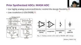
and
Waters
proposed
a
senior
size
ADC
based
on
mesh
architecture
to
increase
the
resolution
of
the
EDC.
However,
the
augmented,
highly
analog
custom
blocks
such
as
op-amp
comparator
and
capacitors,
which
restrict
the
design
flexibility.
D
Also
the
enote
is
still
at
least
the
10
bits.
Another
way
to
enhance
the
resolution
is
used
inside
the
star
architecture,
which
is
proposed
by
Co
and
the
garlic
it
takes
advantage
of
the
source
in
intrinsic
digital
friendly
structure
and
making
the
single
size
flow
to
be
portable
and
robust.
Against
the
input
imperfections.
However,
a
dedicated
cap
compilers
is
needed
for
the
dark
array
leading
to
more
software
complexity.
D
Also,
the
resolution
is
still
limited
by
11
bits
in
not
so
with
the
old
based
ADC,
which
is
highly
digital
and
Senior
size
friendly,
are
naturally
more
compatible
to
synthesize
compared
with
prior
voltage
domain.
Adc
ADC
based
Technologies
ADC,
using
automatic
place
and
raw
tools
is
then
proposed
by
Dr
Lee.
However,
this
inside's
methodology
cannot
achieve
high
resolution
due
to
two
reasons.
First,
is
their
poor
margin
by
automatic
placed
on
the
road
tools?
D
Also
The
Limited
noise
shaping
capability
results
in
a
relatively
low
resolution,
and
maybe
we
will
say
we
can
build
a
higher
order
ADC
to
enhance
the
resolution.
However,
it
Still
Remains
a
loss
of
manual
efforts
to
design
a
new
ADC
for
a
different
resolution
or,
more
importantly,
we
can
say
that
for
different
specifications.
D
D
And
in
this
video
and
from
this
review
we
can
also
see
that
there
are
still
mushroom
for
improvements
in
senior
science
adcs
the
existed,
synthesize
ADC
cannot
demonstrate
smdr
Beyond,
seven
70
DB.
It
is
not
yet
sufficient
to
meet
the
demand
of
many
emerging
applications
such
as
accurate
sensor,
nodes
or
biomedical
circuits,
so
at
least
10
to
20
DB
higher
smdr
is
highly
desired,
but
it
also
makes
automation
even
more
challenging,
because
high
resolution
ADC
tends
to
be
more
analog,
intensitive
and
more
sensitive
to
non-ideality
to
make
the
senior
size
ADC
more
practical.
D
D
So
before
we
talk
about
our
proposed
synthesize
flow
and
methodology,
we
will
firstly
recall
the
general
architecture
of
the
first
order:
noise,
shipping
with
steel
base
ADC.
It
is
consists
of
a
Visio
based
integrator
of
a
phase
domain
quantizer
and
a
dark,
and
in
order
to
achieve
a
very
high
sqlr,
a
high
over
sampling
ratio,
only
called
osr
is
always
demand,
leading
to
limited
bandwidths
of
the
ADC
and
in
order
to
achieve
higher
ISR
with
a
relative,
lower
osr,
a
general
idea
is
to
boost
the
noise
shipping
order
here
on
the
bottom.
D
Here
we
can
see
that
with
cascading
another
vco,
the
ADC
can
achieve
one
additional
noise,
shipping
order
and,
more
importantly,
compared
with
the
first
order.
Adc,
the
extra
blocks,
including
vco,
a
fixed
analyzer
and
attacks,
can
be
shared
with
the
same
library
of
the
first
order,
ADC
in
this
case
batting
extra
vco,
and
this
connector
and
attack
cell
the
noise
shipping
order
can
be
extended
from
first
order
to
a
second
order
or
even
higher
order.
In
theory
providing
a
flexible
trade-off
amount
resolution
bandwidth
and
the
power.
D
This
gives
us
an
inspiration
to
propose
a
single
size,
4
that
use
only
one
universal
library
to
achieve
multiple
specifications
of
the
ADC.
So
here
is
the
detail
of
our
proposed
synthesized
flow.
So
first
we
select
the
architecture
to
realize
the
different
performance
of
the
ADC.
In
this
work
we
synthesize
A
first
order
with
service
ADC
and
a
second
order.
D
Basic
ADC,
using
the
proposed
synthesized
flow
and
the
HDR
generation
step
converts
the
circuits
from
schematic
level
into
gate
level,
dialogue
code
and
this
format
can
be
processed
by
the
digital
automatic
plate
and
resource
talk,
and
notably,
this
process
only
needs
to
be
performed.
Only
one
design.
Other
design
with
different
performance
specifications
can
be
simply
realized
by
directly
editing
the
code
to
modify
the
adc's
parameters,
such
as
noise,
shaping
order
and
the
number
of
the
visual
stages
and
the
library
modification
steps.
D
Augments
The
Foundry
standard
cell
libraries
to
improve
the
adc's
performance,
which
will
be
further
explained
in
the
next
section.
Analogs
analog
customer
cells
is
also
added
into
the
library
and
both
augmented
digital
standard
cells
and
analog
custom
cells
are
then
exported
to
added
to
a
standard
cell
library,
description
fields.
D
In
the
poor,
Plan
Generation
step
a
simple
floor
plan
file
is
written
to
Define
placement
and
the
placement
boundaries
of
the
components
and
the
four
plus
file
along
along
with
the
modified
library
and
HDL
files
as
the
feet
to
a
digital
automatic
plan
and
a
lot
tools
or
record
APR
tools
to
complete
the
layout.
And
in
this
work
we
use
Cadence
nodes
as
APR
tools
by
sharing
the
one-time
setup,
augmented
digital
standard
cell
library
and
the
custom
sale
Library.
D
So
first
and
the
second
order
we
still
base
ADC
are
automatically
synthesized
by
the
APR
tools
from
git
level
available
code
to
a
layout
and
in
summary,
the
proposed
the
CSS
flow
use,
one
universal
library
to
synthesize
adcs
for
multiple
specifications,
and
these
different
specs
can
be
simply
realized
by
editing
the
code
to
modify
the
ADC
parameters.
Therefore,
to
propose
the
synthesized
methodology
quickly,
improves
the
design
productivity,
reduce
the
design
cost
and
shortens
the
product
turned
around.
D
And
obviously,
due
to
this
severe
placement
mismatch
a
huge,
a
huge
rotting
mismatch
is
then
introduced.
This
placement
and
a
rocking
mismatch
quickly
limits
the
adc's,
sndr
and
sfdr
in
order
to
achieve
a
high
resolution.
Adc
a
better
synthesized
methodology
is
strongly
needed,
and
in
this
work
we
propose
a
template
based
synthesized
methodology.
So,
let's
just
think
about
one
question,
so
what
we
will
do
to
achieve
a
high
quality
manually,
craft
CCO
layouts.
D
So
as
a
result,
the
routing
mismatch
is
further
reduced
and
based
on
the
simulation
results.
Thanks
to
the
template
based
place
and
a
road
methodology
we
have
proposed
here,
the
linearity
of
the
CCO
is
improved
by
17
DB,
compared
with
the
methodology
in
Prior
work
and
similar
with
CCO
design.
Without
any
placement
constraint
in
Prior
work,
there
are
severe
Road
mismatch
between
tax
cells.
D
On
the
left
hand,
side
is
the
schematic
of
the
deck
and
for
Simplicity,
only
seven
stage
see
that
unit
cells
are
shown
here
and,
on
the
right
hand,
side.
We
can
see
that
in
Prior
work,
since
there
is
no
timing,
information
included
the
delay
cells
are
placed
without
any
constraint
by
the
APR
tools,
leading
to
a
systematic
mismatch
of
1.3
standard
standard
deviation
for
alternate
Fender
fire
unit
capacitor
unit
capacitors,
due
to
the
rotting
mismatch
and
similar
to
CCO
design.
D
This
worked,
firstly,
synthesize
each
converter,
a
single
size,
each
inverter
and
the
capacitors
in
group,
and
after
that,
the
synthesized
ctac
see
that
elements
are
placed
in
a
row
and
in
this
case
the
road
mismatch
is
greatly
reduced,
leading
to
an
incentralized
zero
systematic
mismatch
amount.
The
unit
capacitors
and,
in
summary,
our
proposed
synthesize.
The
methodology
easily
improves
the
placement
and
routing
machine.
Besides,
since
the
timely
based
cell,
a
one-time
setup
compared
with
prior
work,
the
proposed
technology
as
a
proposed
technique,
as
only
little
manual
effort.
D
And
next
I
will
talk
about
the
circuit
implementation
of
our
proposed
first
loader
and
a
second
order
synthesize
the
order
Thing
by
DC
and
first,
let's
look
at
the
second
implementation
of
the
first
order.
Visual
based
ADC-
and
here
is
the
the
implementation
of
the
vco
and
it
is
implemented
by
a
GM
cell
and
a
pseudo
differential
CCO
pair,
and
here
is
the
schematic
of
the
custom
speed
driven
inverter-based
GM
cell
and
the
GM
cell
directly
drops
two
pseudo
differential
ccos
without
requiring
any
additional
kernel.
D
Source
and
common
mode
feedback
is
not
required
for
the
GM,
as
the
CCO
provides
low
input
impedance,
which
helps
stabilize
the
output
DC
levels
and
the
Toppers
are
introduced
at
the.
It
is
input.
The
output
of
the
GM
cell
and
the
input
of
the
c-dark
and
the
Choppers
is
used
to
mitigate
the
Silicon
wise
and
the
offside
from
the
GM
and
the
deadband
technique
is
also
adopted
to
mute
The
Chopping
transient
and
this
Custom
Custom
switch
are
simply
implemented
by
a
constant,
complementary
switch
pair.
D
Node
is
also
necessary
to
ensure
over
100
DB
sfdr
and
the
double
PFT
based
Quant
header
is
purple,
which
is
proposed
in
2021,
is
adopted
to
provide
full-time
resolution
enhancements
compared
with
the
prior
work,
and
the
double
cavity
based
quantizer
is
also
can
also
provide
see
that
mismatch
medication.
Due
to
its
natural
clock,
averaging
output
pattern
and
the
custom
custom.
The
market,
like
a
level
shifter,
is
used
as
a
CCO
buffer
to
minimize
the
leakage
power.
D
And,
based
on
the
first
order,
first
order,
not
shipping
architecture,
we
add
an
extra
few
videos
and
the
PFT
to
extend
the
noise
shipping
order
to
second
order,
and
an
extra
GM
cell
is
also
introduced
to
ensure
the
stability
of
the
third
Sigma
Loop,
and
the
current
attack
converts
the
phase
difference
of
the
ccos
to
from
phase
domain
to
current
domain
and
thus
summation
with
the
feed
forward,
tm2
output,
currents
and
based
on
the
first
order
and
based
on
the
first
first
order,
ratio-based
ADC.
The
second
order.
D
Visual
base
ADC,
can
share
most
of
the
libraries
except
the
current
current
attack
here.
So
we
can,
but
we
can.
We
should
notice
that
this
one-time
site,
Hub
Library,
can
be
used
to
build
even
higher
noise
shipping
ADC
and
actually,
we
have
implemented
a
third
order.
We
still
based
ADC
by
simply
editing
the
code
based
on
our
existing
work.
However,
the
measurement
result
of
the
third
order
ADC
did
not
achieve
the
performance
as
we
expected,
so
we
did
not
report
this
work
in
this
year's
cicc.
D
And
now
I
will
present
to
you
the
measurement
result,
and
here
is
the
type
photo
and
the
Prototype
first
order
and
the
second
order
ADC
occupies
an
area
of
0.045
and
0.6
millimeters
Square,
respectively
in
28
nanometer
CMOS
process
and
the
Prototype
first
order.
Adc
occurs
at
28.8
megahertz
and
consumes
18
Mega
volts
in
total,
and
the
second
order.
Adc
operates
at
48
megahertz
and
consumes
55
macro
volt
in
total
and
measurement
output,
power.
D
The
response
here
shows
that
the
intermodulation
tool
is
placed
at
over
100
DB
below
the
signal
of
Interest,
which
proves
a
great
linearity
of
the
proposed
ADC
and
for
the
second
order
you
see
at
200,
kilohertz
bandwidth,
the
ADC
achieves
80.2
DB,
sndr
and
96.2s
FDR,
respectively,
and
the
following
test
and
the
inter
modulation
is
placed
at
over
97
DB
below
the
signal
of
Interest,
which
proves
a
great
linearity
of
the
Prototype
BC,
and
the
measurement
result
shows
the
sfdr
and
as
a
sndr
and
SNR.
Of
course,
input.
D
Amplitude
is
shown
here
and
our
work
achieves
a
dynamic
range
of
89.1
DB
for
first
order,
ADC
and
81.3
db4
second
order,
DC
and
under
different
inputted
frequency
from
work.
Your
horse
to
a
20
kilohertz
of
the
first
80s
first
order
ADC
and
one
kilohertz
to
50
kilohertz
of
the
second
order.
Adc,
the
sndr
variation
of
both
ADC
are
within
1db
and
are
both
ADC
shows
a
robust
performance
with
less
than
1.5
DB
sndr
variation
across
six
different
chips.
D
This
work
is
the
first
to
achieve
over
100
and
the
ladbh
raw
form,
among
not
only
student
size,
but
also
manually,
designed,
visual
based
ADC.
This
means
that
our
proposed
senior
size
ADC
is
has
the
quilt
function,
has
the
great
potential
to
put
to
the
Practical
use,
and
this
comes
to
the
conclusion
of
our
presentation
and
in
this
talk,
I
have
present
to
you.
D
and,
as
a
panel
I'd
want
to
mention
a
caveat
and
I
guess.
You
might
already
notice
that
our
single
size
flow
and
the
methodology
seems
only
talking
about
layouts,
so
you
might
ask
how
to
how
about
the
schematic
sizing,
so
how
about
the
simulation
or,
more
generally,
how
about
the
design
closure
so
to
the
to
this
end,
it
is
true
that
our
flow
basically
Focus
just
on
the
layout,
the
closer,
is
still
performance.
D
It's
also
is
still
performed
manually,
but
our
goal
in
this
work
is
try
to
just
make
the
layout
flow
more
streamlined
compared
to
the
existing
work.
In
fact,
we
are
not
losing
any
features,
because
the
design
closure
automation
problems.
It
also
exists
for
other
designs
so,
and
we
also
admit
that
to
ensure
over
100
linearity
of
the
ADC
many
analog
argument
cells
are
added
to
the
library.
D
However,
it
also
should
be
noted
that
once
the
layout
of
the
analog
argument
cells
are
completed,
all
designs
can
share
these
layouts
in
the
library
so
compared
with
full
manually
work,
our
proposed
the
snail
size
flow
still
quickly
reduce
the
memory
effort.
Actually,
we
can
see
that
this
work
tries
to
find
an
optimization
between
the
performance
and
manually
manual
efforts
and
I
think
it
will
be
our
plan
in
the
future
to
look
into
extending
the
automation
automation
to
a
higher
level.
A
E
Yeah
I
was
wondering
if
you
could
share
some
of
the
results
of
your
third
order,
and
if
you
have
any
comments
about
what
makes
the
third
order
or
why
why
the
results
get
worse,
as
you
increase
the
order,
is
it?
Is
it
because
of
the
size
of
the
design
and
the
difficulty
with
the
placement
and
routing.
D
Actually,
the
okay,
so
this
is
a
very
good
question,
so
actually
I
actually
there's
a
trade-off
between
the
thermal
noise
and
and
the
and
the
power
we
we
don't.
We
don't
have
a
very
good
trade-off
of
the
summer
noise
and
the
power
so
for
the
third
order
we
still
base
the
ADC.
The
sndr
is
not
a
shield
as
we
expected,
so
it's
only
7,
70
DB
sndr
at
I.
Remember
is
600
kilohertz
bandwidth.
D
E
A
B
I
just
have
a
question
about
the
the
actual
like
scripting
implementation
that
you
used
for
the
low
level
custom
analog
cells.
I'm
assuming
you
started
probably
from
like
a
a
sized
schematic,
but
then
I'm
curious.
Did
you
use
innovis
at
all
on
those
low-level
design
cells?
Or
did
you
have
some
sort
of
like
skill
or
Open
Access
interface
in
order
to
generate
the
the
unit
cells
for
the
layout.
D
Oh
okay:
okay,
thanks
for
our
question
and
yes
for
for
this,
this
an
analog
part.
Actually,
we
we
do
it
just
for
manually
design,
but
actually
this
this
analog
part.
It
is
not
very
difficult
to
to
design
this
analog
called
part,
because
this
gmsl
is
just
a
inverter-based,
the
GM
cell-
and
this
is
also
just
a
basic,
complementary,
complementary
switches,
and
this
this
is
just
the
Classic
bootstrap
switch
and
I
I
I
admit
that
it.
D
C
A
A
I
mean
they
are,
they
are
not
I,
mean
I,
understand
abstract
from
the
issue
right,
like
those
cells
need
required
from
high
attention.
So
you
spend
a
good
time
doing
that.
So
how
do
you
iterate
in
your
design,
right,
you're
gonna,
make
a
lot
of
the
blocks
are
automated
and
then
you
create
the
first
version
of
the
GM
cell
and
then
you
build
I'm
guessing
you
build
everything
together.
So
so
what
is
the
process
and
how
much
time
does
it
require
to
do
this.
D
D
D
D
B
A
A
D
D
C
A
Yeah
so
we'll
open
up
this
operation,
18p
cells
I
mean
not
the
GM
cell,
like
the
whole
GM
cell,
but
we're
trying
to
build
a
little
more
than
one
transistor,
multiple
transistors
as
P
cells
and
we're
trying
to
build
more.
You
know
customized
circuits
like,
but
it
feels
like
taking
a
whole
cdap
or
a
GM
cell
as
a
P
cell
and
import
it
across
different
nodes
can
take
a
lot
of
time
to.
C
A
D
A
All
right
so
I
guess
that's
about
it
thanks
so
much
he
and
welcome
to
the
analog
working
group.
Okay!
Well,
there's
a
couple
updates:
we
were
working
on
on
the
with
the
students
from
the
Google
summer
code,
so
hopefully,
in
the
next
week
they
can
provide
the
updates
on
their
framework.
They
are
building
with
GDs,
Factory
and
open
road.